













'Beyond human intuition': AI designs chip components 500 times smaller than what engineers could ever imagine
Three new AI-designed chip components are just a few micrometers long and go beyond what human engineers have previously envisaged.


Photonic microchips are around the size of a penny. This close-up shows computer-designed nanostructures, wavelength splitters, mode sorters and mirrors, while the illustrations on the left show how the components could be integrated into photonic circuits.
Scientists have successfully shrunk three components used in photonic microchips by up to 500 times, leaving considerably more space for other on-chip functionality. The achievement was made possible with an artificial intelligence (AI) algorithm that generated these tiny designs, which the researchers described as "beyond human intuition."
Whereas conventional microchips use electrons to transmit and process information, photonic microchips utilize particles of light (photons). They can therefore process and transmit data much faster than electronic chips can, because photons can carry information at the speed of light. They also offer higher bandwidth, as different wavelengths can carry distinct data streams, and they lose less energy as heat.
As a result, photonic chips are used where fast, high-bandwidth data transmission is essential, such as in fiber-optic communications, data centers, AI, lidar systems for autonomous vehicles, and quantum computing.
Instead of metal wires, micrometer-wide channels called waveguides direct light across the photonic chip. These chips also contain wavelength splitters, spatial mode sorters and mirrors — all of which are essential for separating and directing different wavelengths and light patterns within a footprint a fraction of the width of a human hair.
In the new study, the scientists used AI-generated designs to fabricate these three components on an ultracompact scale. They published their findings May 28 in the journal Nature Communications.
The newly available on-chip space could allow engineers to "unlock new functionalities" by packing on more components, the researchers wrote in the study. Notably, the work demonstrates that AI can produce boundary-pushing chip designs that are also practical to manufacture.
AI worked backward to generate the component designs
The researchers started by informing the algorithm exactly what they wanted the components to do to the light and by providing certain manufacturing constraints, such as limits on how sharply the nanostructures could curve
Get the world’s most fascinating discoveries delivered straight to your inbox.
The AI algorithm then worked backward, testing and refining different designs until it found the delicate nanostructures that could achieve the desired result.
"Inverse design lets us define what we want light to do, and the optimization finds a structure that does it, often one no human would have drawn," study first author Toby Bi, a researcher at the Max Planck Institute for the Science of Light, said in a statement. "What is exciting is that the same framework can do three quite different jobs on the same chip: route light by wavelength, sort it by spatial mode, and act as compact mirrors that form on-chip optical cavities."
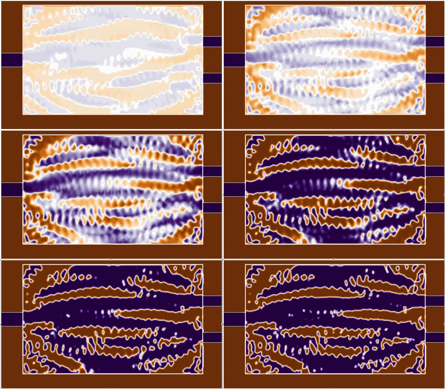
The components were designed by an AI algorithm that refined their geometry through iterative optimizations for use in photonic circuits.
Components for photonic chips typically have hand-engineered designs. Engineers start with a tried-and-true design and painstakingly optimize it for new performance parameters. On top of being slow, this method limits the range of device geometries that can be explored.
To improve their components further, the team also opted to create the components out of relatively thick silicon nitride — roughly 400 to 800 nanometers thick, compared with 150 to 400 nanometers for standard silicon — which wastes less light and offers stronger wavelength confinement.
The resulting mirrors, which are about 11 μm long, reflected up to 98.5% of incoming light while blocking unwanted light patterns. When placed in pairs on each side of a waveguide, the light bounced between them over 100 times before escaping, demonstrating the silicon nitride's low losses, the scientists explained.
The wavelength splitter is roughly the size of a single bacterium (approximately 5 μm across), and the spatial mode sorter is marginally larger.
AI-designed chips edge closer to real-world use
While the researchers have successfully demonstrated these compact components individually, they have not combined the components into a complete integrated optical circuit yet. Achieving this will be the next step toward building fully functional photonic chips that harness the increased component density enabled by these designs.
Related stories
- Scientists figured out how to shrink huge ultrafast lasers so they fit on a tiny chip — the 'holy grail' of the field
- Breakthrough in experimental light-powered quantum computers could mean scaling them up is now far more viable
- New wonder material designed by AI is as light as foam but as strong as steel
"These results demonstrate the feasibility of compact, fabrication-error-robust, customised photonic components and pave the way for scalable, high-performance integration in silicon nitride-based photonic systems," the researchers wrote in the study.
In recent years, engineers have begun exploring how AI can be integrated into the semiconductor design and fabrication pipeline. In the past, AI-driven approaches have reduced design cycles from weeks to hours while significantly lowering manufacturing costs.
Some systems can even generate effective chip designs from a 200-word prompt. Google's AlphaChip, a machine learning method that designs chip layouts, has produced "superhuman" floor plans that have been deployed in the tech giant's production AI chips.
Bi, T., Zhang, S., Bostan, E., Liu, D., Paul, A., Ohletz, O., Harder, I., Zhang, Y., Ghosh, A., Alabbadi, A., Kheyri, M., Zeng, T., Lu, J., Yang, K., & Del’Haye, P. (2026). Inverse-designed silicon nitride nanophotonics. Nature Communications, 17(1). https://doi.org/10.1038/s41467-026-73390-9

Fiona Jackson is a freelance writer and editor primarily covering science and technology. She has worked as a reporter on the science desk at MailOnline, and also covered enterprise tech news for TechRepublic, eWEEK, and TechHQ.
Fiona cut her teeth writing human interest stories for global news outlets at the press agency SWNS. She has a Master's degree in Chemistry, an NCTJ Diploma and a cocker spaniel named Sully, who she lives with in Bristol, UK.
You must confirm your public display name before commenting
Please logout and then login again, you will then be prompted to enter your display name.