
 Live Science Plus


Nanobots Bedazzled with Diamond Parts

Wear and tear presents a unique problem for microscopic nanobots. Unlike their larger relatives, handymen can't simply swap a spare part into a machine that's the size of a red blood cell. The solution? Make micro-electromechanical systems (MEMS) from diamonds, since nothing resists daily wear better than the world's hardest substance.
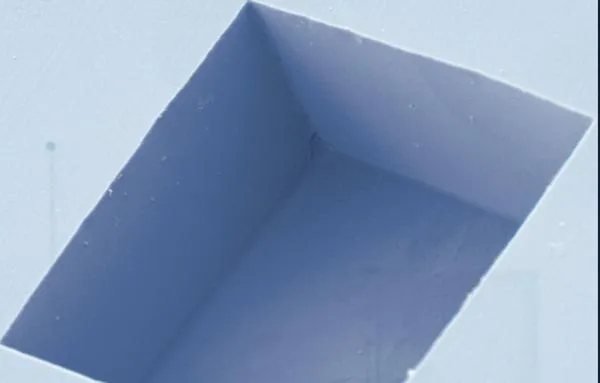
Scientists at the National Institute of Standards and Technology (NIST) have figured out how to do just that, etching microscopic, box-shaped pits into diamond using corrosive chemicals. The divots are so exact that they could easily become the teeth of gears, or some other component of a nanoscale machine.
"Diamond may be the ideal substance for MEMS devices," said Craig McGray, a researcher at NIST. "It can withstand extreme conditions, plus it’s able to vibrate at the very high frequencies that new consumer electronics demand. But it's very hard, of course, and there hasn't been a way to engineer it very precisely at small scales. We think our method can accomplish that."

The method uses a chemical etching process to create cavities in the diamond surface. The cubic shape of a diamond crystal can be sliced in several ways — a fact that jewelers take advantage of when creating facets on gemstones. The speed of the etching process depends on the orientation of the slice, occurring at a far slower rate in the direction of the cube’s "faces"—think of chopping the cube into smaller cubes—and these face planes can be used as a sort of boundary where etching can be made to stop when desired.
In their initial experiments, the team created cavities ranging in width from one to 72 micrometers, each with smooth vertical sidewalls and a flat bottom. For comparison, a human hair is about 100 micrometers thick.
"We'd like to figure out how to optimize control of this process next," McGray said, "but some of the ways diamond behaved under the conditions we used were unexpected. We plan to explore some of these mysteries while we develop a prototype diamond MEMS device."
This story was provided by InnovationNewsDaily, a sister site to Live Science. Follow InnovationNewsDaily on Twitter @News_Innovation, or on Facebook.
