Tiny Microchip Component Promises Big Returns

Get the world’s most fascinating discoveries delivered straight to your inbox.
You are now subscribed
Your newsletter sign-up was successful
Want to add more newsletters?
Join the club
Get full access to premium articles, exclusive features and a growing list of member rewards.
This Research in Action article was provided to Live Science in partnership with the National Science Foundation.
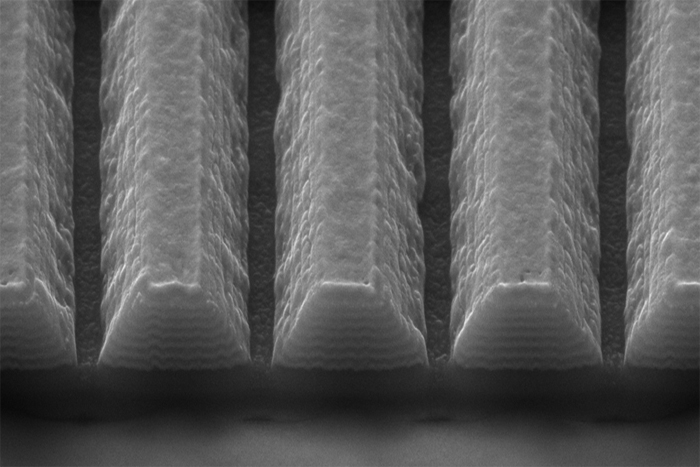
Although smaller than the width of a human hair, a light-absorbing microchip component promises to provide a big return on performance for solar cells, consumer electronics and even stealth technology. The nanoscale waveguide taper array slows light over a broad range of wavelengths. No small feat, especially since light travels at 300,000 kilometers per second and previous attempts could slow light only over a narrow range of wavelengths.
The taper array comes after five years of theoretical and experimental work by Qiaoqiang Gan, first as a graduate student in Filbert Bartoli' group at Lehigh University and then as a professor at the University at Buffalo, The State University of New York. Gan's efforts resulted in a carefully crafted ultrathin film composed of multiple layers of metal, semiconductor and insulating materials. By etching specific patterns into the layers and adjusting their thickness, the array can absorb a "rainbow" of wavelengths. This will allow for more efficient energy absorption for a number of applications.
Article continues belowIn the field of solar energy the array will allow photovoltaic cells to store all of the wavelengths in the solar spectrum. Current cells based on semiconductor materials only absorb specific portions of the solar spectrum. The ability to tune the array across the spectrum also makes it attractive as a device to recycle thermal energy. When integrated with devices that give off heat and radiate electromagnetic waves , the array could help recycle the heat into electricity, improving the performance of a range of devices including consumer electronics.
In the case of optical communications, the array could eliminate noise created by unwanted signals on circuits or in optical channels. In the military arena, when incorporated into military vehicles, the array technology could act as a cloaking device allowing the vehicles to avoid radar, sonar or other forms of detection.
Gan and his colleagues use techniques called sputtering and evaporation to deposit alternating layers of silver and silicon dioxide thin films on a substrate. The researchers then carve out the array on the multilayers with ion beam lithography, a technique that uses ions to transfer the tapered pattern onto the multilayers. By adjusting the thickness of the layers and the shape of the patterns, the researchers determine the array's optical properties.
"The surprising aspect of [this technology] is our ability to design optical absorption over an ultrabroad spectrum," says Gan. "We can tune the absorption of the patterned [array] to any wavelength, from the visible to the microwave region and even finely manipulate the absorption profile to mimic natural materials."
Get the world’s most fascinating discoveries delivered straight to your inbox.
Editor's Note: Any opinions, findings, and conclusions or recommendations expressed in this material are those of the author and do not necessarily reflect the views of the National Science Foundation. See the Research in Action archive.
 Live Science Plus


